

LED Displays Are Going To Get Much Clearer Thanks To A Plasmonic Cavity
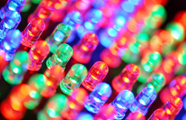
A plasmonic cavity sounds like technobabble straight out of an episode of Star Trek, but it could be the key to making LED displays clearer and more efficient. The plasmonic cavity is a nanostructure originally developed by Stephen Chou of Princeton University to boost solar power efficiency, but he realized it might have applications in emitting light as well as absorbing it. That could mean better screens on your devices.
One of the fundamental problems with LEDs is that they have a solid structure that traps most of the light they produce. On average, only 2-4% of the light generated by an LED actually makes it out. Chou says the use of plasmonic cavities could boost that by four times. There are methods now that can make organic and inorganic LED displays brighter by increasing light output, but they come at the cost of reduced contrast. A plasmonic cavity shouldn’t come with that drawback.
So what is a plasmonic cavity? It’s a nano-scale structure composed of a 100 nanometer thick light emitting surface between two cavities. On one side is a thin metal film and on the other is a mesh of thin metal wires. This is called a plasmonic cavity with subwavelength hole-array (PlaCSH). It takes advantage of plasmonics, a set of effects observed in the density of electrons generated when photons hit a metal surface. This design essentiallyguides the light out of the LED toward the viewer. This could make displays much clearer, but also reduce power requirements as more energy is turned into usable light instead of lost.
Fabricating these structures isn’t even very expensive–it can be done with technology that is already in use. Princeton has already filed for patents on both organic and inorganic LEDs based on PlaCSH.

You may also like...


![]() © 2024
© 2024
0 comments